On April 21, 2022, the OnePlus TWS Bluetooth earbuds Buds N was officially marketed. It has excellent performance such as 12.4mm super-large moving coil Dolby Atmos, 7 hours of continuous listening at a time, an accumulated 30 hours of ultra-long battery life, and 94ms of ultra-low latency of Bluetooth 5.2. Thinkplus Semiconductor provides OnePlus Buds N with integrated solution of power management, including TWS earbuds power management IC SY8801, power management IC SY5501 and OVP IC SY8702, helping OnePlus to provide users with excellent product experience.

About SY8801
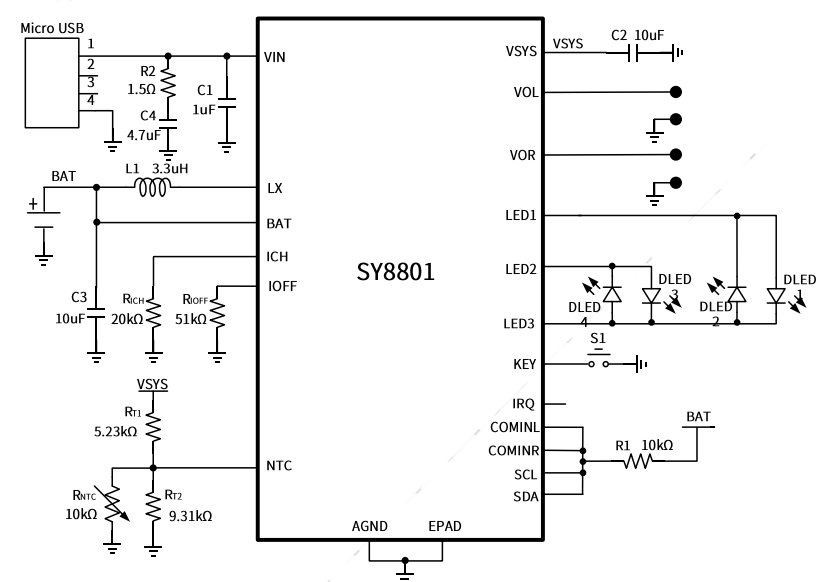
SY8801 is a single IC solution specifically designed for TWS cradle with an integrated charging and discharging module, charge current and discharge termination current are externally adjustable; output power supply and ground are used to achieve communication between the earbuds cradle and the earbuds. The IC uses standard I2C interface and interrupt signal to realize fast communication between IC and MCU. At the same time, the IC also has load detection and load insertion identification functions. SY8801 is well matched to the design of the TWS earbuds cradle, greatly simplifying peripheral circuits and components, and providing an easy-to-use solution for application of TWS earbuds cradle. SY8801 is available in a QFN24 package.
Applications
l TWS earbuds cradle and portable electronic devices
Features
l Standby current: < 5uA
l Adjustable charge current via external resistor, and constant VIN current
l 1.2 A maximum charge current
l Up to 28V absolute maximum input voltage
l 93% discharging efficiency @0.5A
l Charging-discharging path management, discharge first
l Preset 4.2V/4.35V floating charge voltage with ±1% accuracy
l 5V synchronous boost output with efficiency up to 93% @ 0.1A.
l Load insertion identification
l Load current detection and adjustable low-load shutdown current via external resistor
l Over-current, short-circuit, over-voltage and over-temperature protections of discharging module
l 1-4 LEDs for external automatic identification; earbuds insertion prompt
l Start/stop of discharge by clicking or long pressing KEY (optional)
l VOL/VOR supports two single-line communication modes
l Enable control and I2C communication interface, flexible product customization.
l Compliance with the latest IEC62368

(Typical Application Circuit)
About SY5501
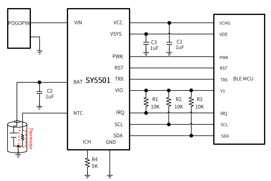
SY5501 is specially designed for TWS earbuds, providing a perfect solution for charging and isolated communication. It integrates linear charger, discharge protection, single-line bidirectional data communication between cradle and earbuds and I2C communication interface to allow for charging-discharge management and protocol communication. It supports adjustment of maximum charge current via external resistor, and of constant current charge ICC and floating charging voltage (VFLOAT) I2C. The integrated NTC ensures safer charging and discharging of the battery. The battery discharge protection and ship mode ensure low power dissipation of earbuds system. The private control command is sent from the earbuds cradle via VIN to control the IC, so as to turn on / off and reset the master of earbuds. SY5501 also supports the identification of earbuds in or out of the cradle and issues a notification to the master. Multiple functions and low power dissipation ensure a shorter development cycle for Bluetooth earbuds. The simplified 1.6mmx1.6mm QFN14 package greatly saves space for Bluetooth earbuds solution.
Applications
l TWS earbuds, Augmented Reality goggles and portable electronic devices
Features
l 1uA VBAT standby current
l 300 nA current in ship mode
l VIN withstand voltage=12V, VIN OVP = 6V, over-current protection=450mA
l Adjustable charge current via ICH pin within the range of 10-300mA at 8 levels by percentage.
l Adjustable floating charge voltage 4.2/4.35/4.4/4.45V, with ±0.5% accuracy
l Separately adjustable trickle current and termination current
l Active recharge with multiple levels of adjustable voltage
l Integrated NTC detection for JEITA temperature interval protection
l Integrated over-voltage, over-temperature and timeout protection of rechargeable battery
l Integrated under-voltage, over-current and short-circuit protection of discharged battery
l Integrated two-way communication, automatic switching of communication direction at a rate up to 3Mbps
l Integrated private protocol command for chip control by commands from cradles via VIN
l Integrated in-cradle/out-of-cradle detection by sending a reset or wake-up signal to Bluetooth master respectively
l I2C control, status reading, and interrupt output

(Typical Application Circuit)
About SY8702
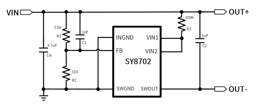
SY8702 is a low side Over-Voltage-Protection (OVP) IC. It internally integrates NMOS switch with an internal resistance of 28mΩ, and uses low-voltage side switch topology and ultra-low on-resistance for more flexible application, which can effectively reduce the input voltage drop, and protect voltage external setting. All this makes SY8702 the simplest and the most practical low-cost OVP solution. SY8702 is available in a SOT23-6 package.
Features
l Overvoltage protection point up to 36V
l External setting of overvoltage protection point
l Switching NMOS with an internal resistance of 28 mΩ
Applications
l Mobile devices such as power bank, mobile phones, tablet PCs and electric tools

(Typical Application Circuit)
Thinkplus Semiconductor has been deeply cultivated in the field of power management technology, and committed to providing leading battery management system level IC solutions for industries such as smart wearables, consumer electronics, industry, energy storage systems, and new energy vehicles, which makes it win the trust and praise from customers. Thinkplus Semiconductor will launch more product portfolios and better solutions to bring better product experiences to global consumers in the future.
Previous articleThinkplus Semiconductor Boosts Launch of OPPO Enco Air2 Pro with a Power Management System2022.04.25
Next articleNew Product | Thinkplus Semiconductor Launches 2A BUCK Charger IC SY6201 with 10mA Termination Current2022.03.26